How to Choose a 3D SPI Machine
What to check when specifying a 3D solder paste inspection machine: the measurements and defects it must catch, resolution versus speed, board envelope, warpage compensation, software and closed-loop evidence.
6 min read
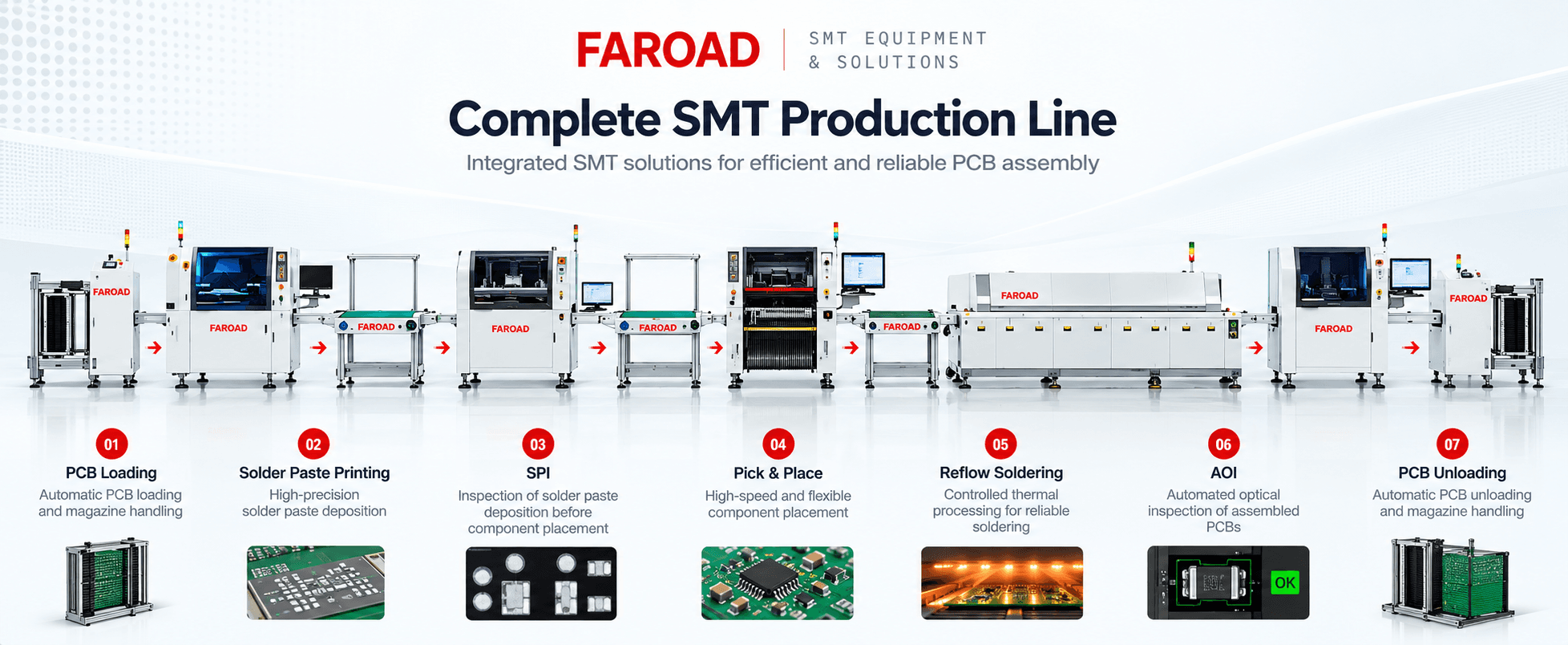
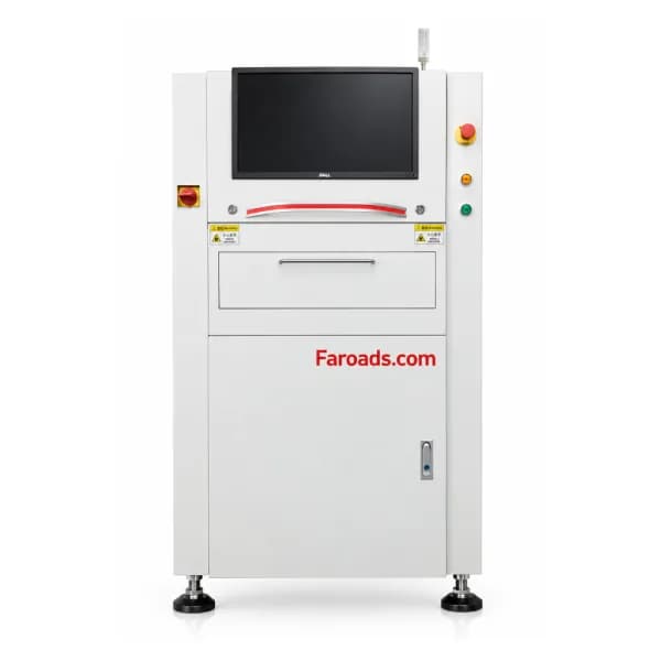
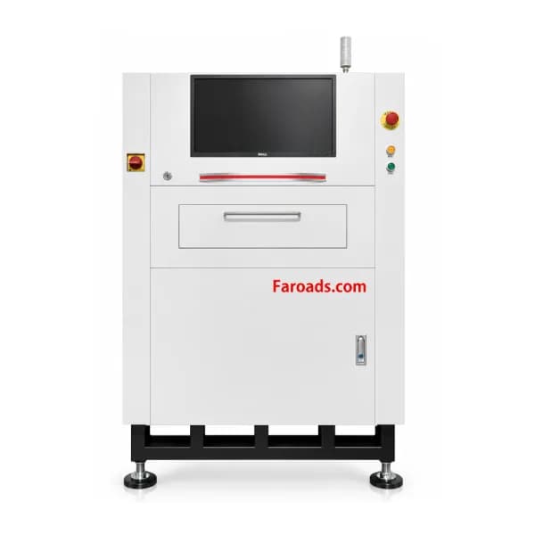
A 3D SPI machine inspects the solder paste deposit after printing and before placement. The buying decision covered here is how to specify that machine: what it must measure, how fast and how fine, what board size it must hold, and which software and feedback functions you should verify.
This is not a guide to whether you need SPI versus AOI, and it is not a guide to purchasing the printer and the inspector as one package. Those questions are covered in SPI vs AOI and in buying a printer and SPI together.
FAROAD lists a 3D SPI for PCB inspection. The listed AOI machines are 2D, and we do not treat them as a 3D SPI substitute. The figures below come from the live 3D SPI inspection machine page, re-checked on 17 November 2026. Confirm the configured options in your quotation.
What a 3D SPI actually measures
A 3D system is useful because paste quality is not only "present or missing." The FAROAD SPI page states that the machine measures solder paste volume, area, height, XY offset and shape. Those five results tell you whether the deposit is short, tall, shifted or badly formed before a component is placed.
The same page lists the defect classes the inspection is intended to flag: missing printing, insufficient solder, excessive solder, bridging, offset, malformed shapes and surface contamination. That list is a coverage check, not a promise that every escape will be caught. You still have to set thresholds against your paste and pad design, and you should trial the pads that actually fail in your process — close-pitch devices, small chip components, large ground pads and any deposit next to a via or mask feature that confuses a weaker system.
The page also describes RGB 2D lighting used together with the 3D measurement, including on boards of different solder-mask colors, as a way to stabilize height, volume and area results. Ask to see that behavior on your mask color, not only on a demonstration board.
Resolution, speed and the board envelope
Finer resolution is not automatically better if it slows the machine below the printer. The live product page lists several lens resolutions in the specifications table and, in the feature text, a wider set of example values. Those two lists are not identical, so do not treat a single brochure figure as the configured machine. Ask the supplier to state the lens resolution, field-of-view size and inspection speed for your finest pads, and to show how that speed compares with your printer cycle.
The specifications table quotes 0.35–0.5 s for each camera field and 0.3 s to inspect one mark. Convert those times into a board cycle only after you know how many fields your panel requires. A long or densely padded board can need many fields; a short cycle on a small demonstration panel will not apply.
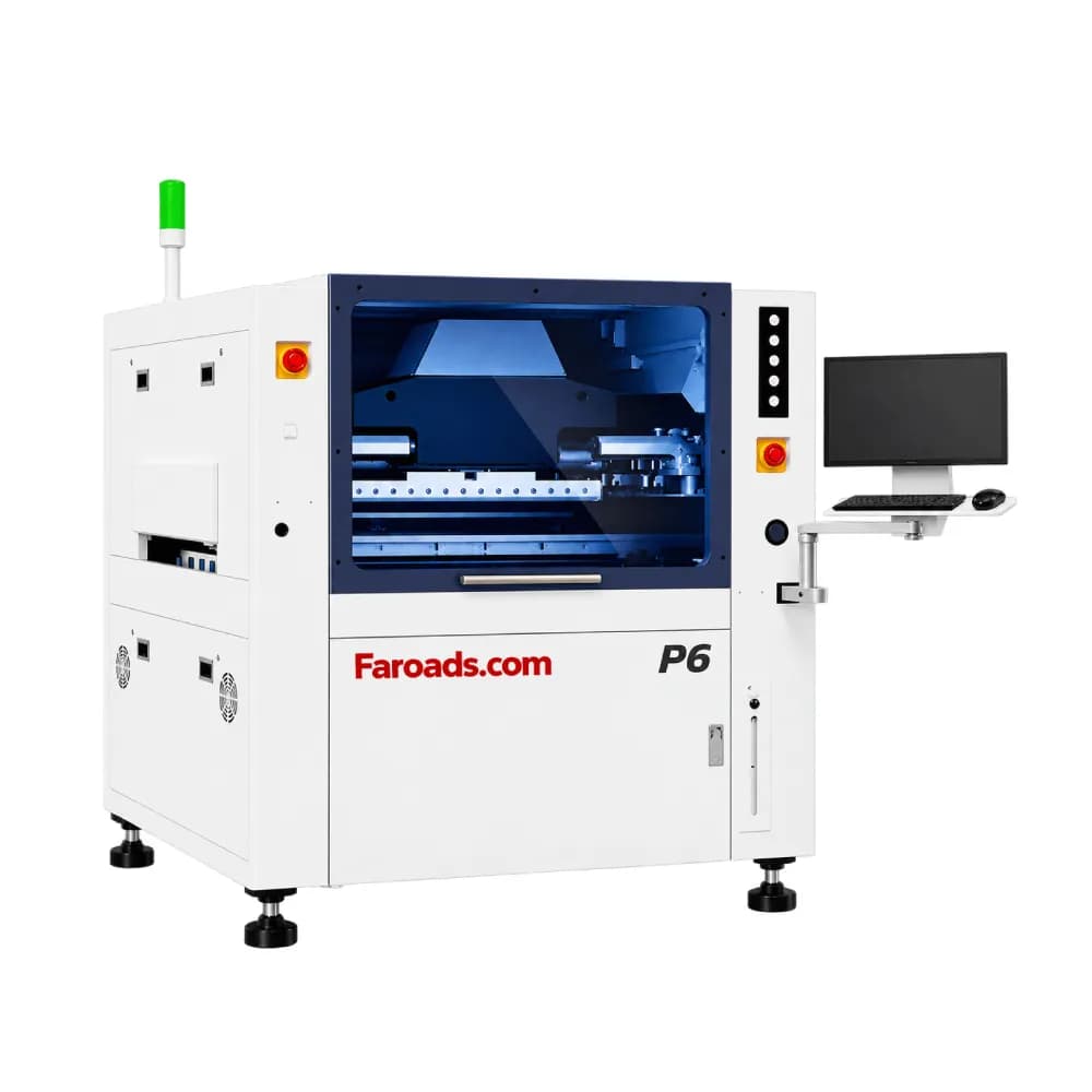
Match the mechanical envelope as carefully as the optics. The FAROAD SPI page lists 450 × 500 mm as the largest board it can load and inspect. That is smaller than some FAROAD printers — the P6 page lists a maximum substrate of 650 × 610 mm, expandable to 750 × 610 mm. If you print large panels, confirm that the SPI can accept the same width and length, or plan a process limit. Also confirm transport direction, track-width adjustment and any rear-fixed-track option you will need to match the line.
Warpage compensation and inspection height
Thin, flexible or already-bowed boards are a frequent source of false calls and missed defects. On bowed or flexible boards, the FAROAD SPI page describes a warpage-correction scheme that uses a moving Z-axis adjustment together with a fixed correction in the telecentric optics. It also publishes a warp-height measuring range of ±5 mm. Test those claims on your most bowed production panel, not a flat coupon.
Separately, the standard maximum measuring height for the paste deposit is listed as ±550 μm, with ±1200 μm as an option. If you print taller deposits, or you need to clear unusual board features, confirm which height range is in the quoted configuration. Optional minimum-component packages (the page lists 01005 / 03015 / 008004 as options) should be treated the same way: include them only if your product mix requires them, and then trial those parts.
Programming, SPC and line data
A machine that is slow to program will not be used on every job. The FAROAD page lists GERBER import and a programming interface aimed at faster program creation, plus offline programming as an option. In the trial, time how long it takes to build and verify a program from your real data, including any manual cleanup around unusual pads.
SPC should be more than a live chart on the operator screen. The page describes real-time SPC display, quality-control tools and multiple data-output formats, with SPC software also listed among the options. Ask which statistics you will actually export, and whether the system can store results by program, lot and board serial if you need traceability.
MES access is listed as a capability, with multiple data-format interfaces for uploading inspection data. If you already have a manufacturing or quality database, make the data format and the handshake part of the purchase discussion. The page also describes combining SPI results with AOI measurements taken before and after the oven. That is a line-level quality loop. It is not a reason to treat AOI and SPI as interchangeable tools.
Closed-loop to the printer: a capability to verify
The FAROAD SPI page states that results can be sent to the printer and the mounter so those machines can adjust the process, and that the system can identify marks and bad marks automatically. Closed-loop feedback is valuable when it actually changes a printer offset or alerts an operator before a long run of bad prints. It is not automatic just because a brochure mentions it.
Agree what the loop will do — offset correction, a process warning, or both — how the two machines will be connected, and how you will demonstrate it on your printer. Use our pairing article when you are scoping a joint printer-and-SPI purchase. Use the checks above when you are specifying the SPI itself.
Frequently asked questions
Is a printer's 2D paste camera enough instead of a 3D SPI? A 2D check can catch missing or badly shifted prints. It does not measure height and volume the way a 3D SPI does. If those measurements matter to your yield, specify 3D.
Should I always choose the finest resolution? No. Finer resolution usually means more fields or a longer cycle. Choose the resolution that inspects your smallest pads reliably at a speed the printer can feed.
What if my boards are larger than 450 × 500 mm? Treat the published 450 × 500 mm envelope as a hard check. If your panels are larger, ask whether a different configuration exists or whether the process must stay inside that size.
Does closed-loop feedback replace process engineering? No. It can correct small, repeatable offsets faster than an operator can. Stencil condition, paste condition and printer setup still have to be right.
Request a 3D SPI specification review
Send FAROAD your panel size, finest pads, line cycle and any bowed or flexible boards you inspect. We will propose a 3D SPI configuration and a trial that measures the deposits you actually print. Request a quote to start that review.