5G PCB Assembly: What Your SMT Line Needs to Handle
What makes 5G and communication boards harder to assemble, and how to judge printing, placement, reflow and inspection equipment for RF modules, shielded boards and dense radio arrays.
5 min read

5G infrastructure and devices have changed what a typical communication board looks like. Radio modules for millimeter-wave bands, dense antenna arrays, small cells and compact IoT modules all pack more parts into less space, often under metal shields. For the assembler, the challenge is less about exotic machines and more about holding a tight process across every step of the line. This guide explains what to check on each type of equipment when 5G and communication boards are part of your plan.
What makes 5G boards harder to assemble
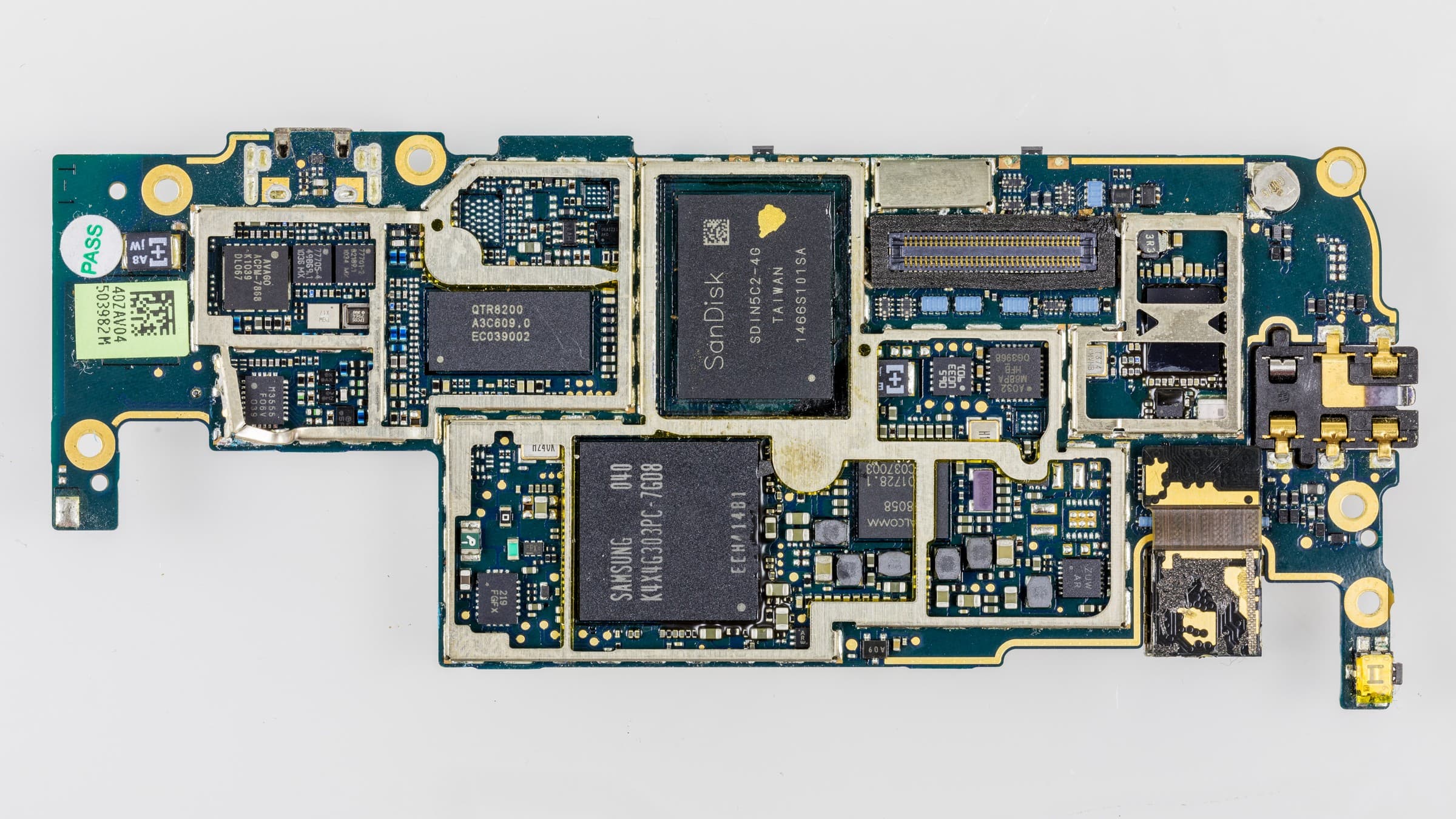
A smartphone main board with its RF shield covers removed, showing the shield frames, chip passives and fine-pitch packages typical of compact communication boards. © Raimond Spekking / CC BY-SA 4.0 (via Wikimedia Commons). Source on Wikimedia Commons, CC BY-SA 4.0. Resized from 6332 × 3562 px to 2400 × 1350 px and recompressed as JPEG for publication; not cropped. This file is shared under the same license.
FAROAD's 5G and communication pages describe the main product groups: millimeter-wave modules with amplifiers and switches for the 26, 28 and 39 GHz bands, massive MIMO antenna boards with dense RF arrays, outdoor base stations and small cells, and compact 5G phones and IoT modules. From an assembly point of view they share several traits:
- Very small passives placed close together, so print and placement errors quickly cause bridging or tombstones.
- Fine-pitch and bottom-terminated packages, such as QFNs, LGAs and BGAs, whose joints are hidden after reflow.
- Shield cans and frames that cover sections of the board and are placed late in the sequence.
- Mixed thermal mass, with large shields and connectors beside tiny chips.
- Specialized laminates on some RF boards, which may behave differently from standard FR-4 during reflow.
Because RF performance depends on consistent joints, small variations that would be tolerable elsewhere can affect the finished product.
Printing: control the smallest deposits
Small passives and fine-pitch packages need small, consistent deposits. That puts weight on stencil design, board support and printer alignment. An automatic printer with vision alignment, closed-loop compensation and an under-stencil cleaning system is the baseline. A 3D SPI after the printer is strongly advisable for this work, because it measures every deposit before parts hide it. FAROAD's Inpex 510 3D SPI lists volume, area, height, offset and shape measurement and closed-loop data sharing with printers and placement machines.
Placement: small chips and large shields on one board
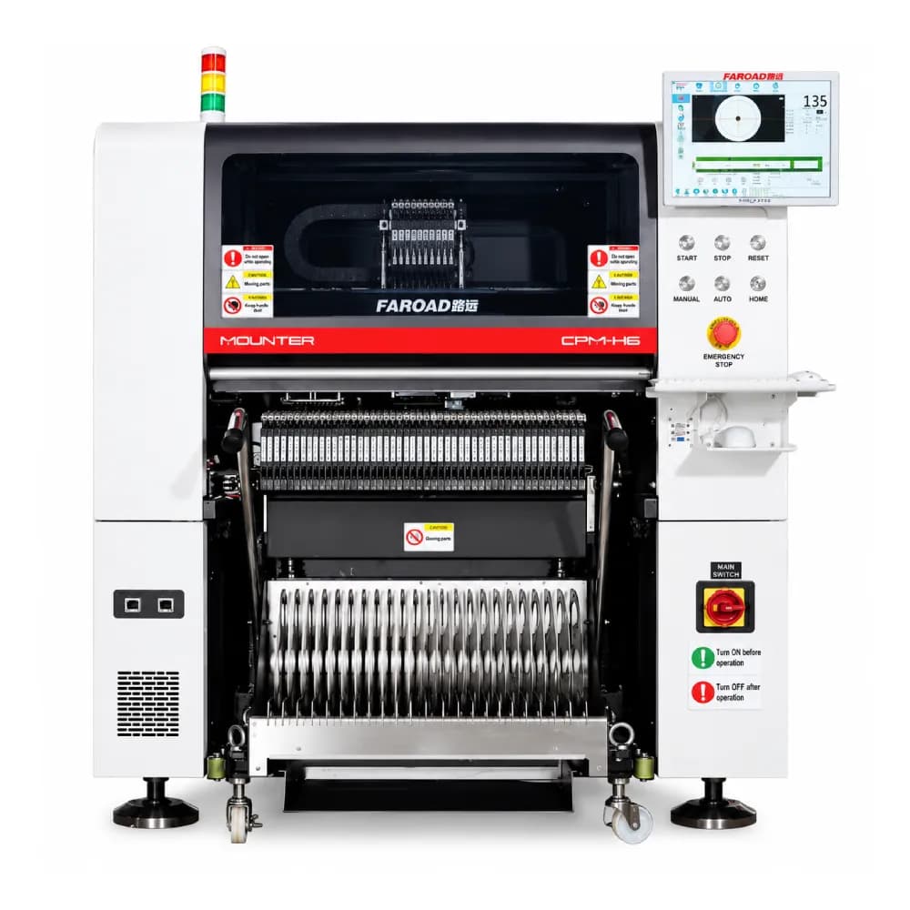
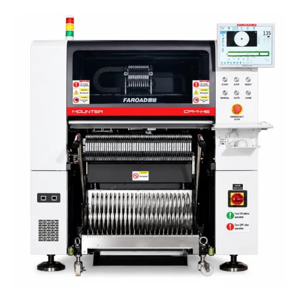
A 5G board often combines the smallest chips with large shield frames, connectors and RF modules, so the mounter needs both precision and range. The CPM-H6 is the model FAROAD shows on its 5G page. It lists:
- 90,000 CPH optimal speed in its high-speed configuration, using dual arms and a dual-track conveyor.
- Placement accuracy of ±0.035 mm (high-speed) and ±0.03 mm (multi-functional), CPK ≥ 1.0.
- Flying-camera recognition from imperial 0201 chips to 12 × 12 × 6.5 mm packages, plus fixed-camera handling of larger parts (as big as 55 × 55 × 25 mm) when configured as a multi-functional machine.
- Single-track boards as large as 510 × 510 mm, between 0.5 and 9.0 mm thick.
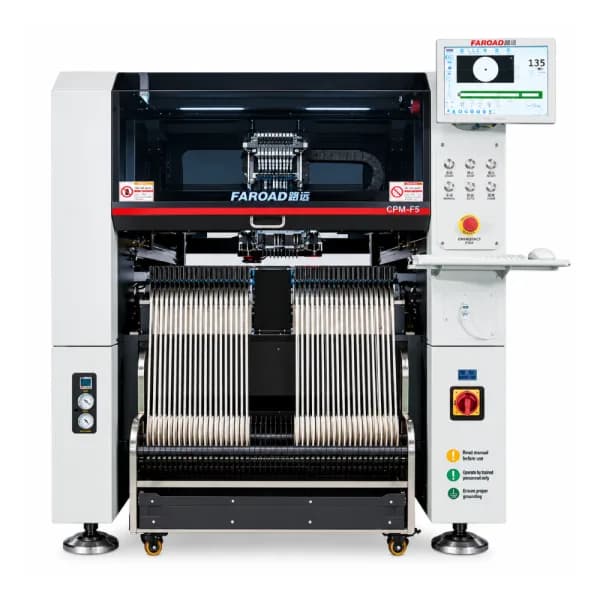
Where boards need only small parts but very fine accuracy, the CPM-HX40 lists ±0.025 mm, although its listed component range stops at 6 × 6 × 3 mm, so large shields would need another machine. Ask your supplier to place your actual shield frames and smallest passives during evaluation, and check how shields are fed, whether by tray, tape or stick.
Reflow: uniform heat and controlled atmosphere
Large shields absorb heat while tiny chips heat quickly, so the oven must keep temperature differences across the board small. Profile with thermocouples on a shield, under a BGA or LGA, and on the smallest passive. Hidden joints under bottom-terminated parts are sensitive to voiding, and many communication assemblers use nitrogen to improve wetting.
For atmosphere control, the N versions of FAROAD's MS-series ovens come with oxygen measurement, nitrogen flow metering and an external water chiller, and the series recovers nitrogen from exhaust gas. Our article on nitrogen reflow oven investment explains when nitrogen pays for itself.
Inspection: plan for what AOI cannot see
FAROAD's current AOI machines are 2D. They check visible parts and joints after reflow, including missing parts, offset, tombstoning and bridges, but they cannot see joints under BGAs, LGAs or soldered shield cans. For those, assemblers use X-ray inspection. X-ray is listed as a coming-soon category at FAROAD, so plan that capability separately. A practical approach is to inspect sections before shields are placed where the process allows it, and to use SPI data to keep print quality under control before joints are hidden.
Run a qualification build before volume
Communication customers often ask for evidence that a line can build their board consistently before they release volume orders. A short qualification build gives you that evidence and tests the equipment at the same time:
- Print a set of boards and review SPI results on the smallest apertures.
- Place parts, then stop a few boards before reflow to check offset on the tiniest chips and the alignment of shield frames.
- Reflow with a profiled board and record the result for each product.
- Inspect with AOI, then send sample boards for X-ray or cross-section where hidden joints matter.
- Record defects by type and station, adjust, and repeat until results are stable.
The same records become the baseline for future builds. When a problem appears months later, you can compare current SPI, placement and profile data with the qualified state rather than starting from nothing.
Questions to settle before you buy
- What is the smallest passive and the finest-pitch package on your roadmap?
- How large and how heavy are the shield frames, and how are they supplied?
- Will boards be shielded before or after inspection?
- Do any laminates require special profile limits?
- What records do your customers expect per board?
Frequently asked questions
Do 5G boards need a special pick-and-place machine? Not usually. They need a mounter with fine accuracy for small passives and enough range for shields and connectors, which many modular machines provide. Is nitrogen required for 5G assembly? Not always, but many assemblers use it for fine-pitch and hidden joints. Test your boards with and without nitrogen before deciding. Can AOI inspect under shield cans? No. 2D AOI sees only visible joints. Hidden joints need X-ray or inspection before shields are fitted. Is SPI worth it for communication boards? For boards with very small passives and fine-pitch packages, SPI is one of the most effective ways to prevent defects early.
Plan a line for your communication boards
Share your board sizes, smallest components, shield types and volumes with FAROAD, and our team will suggest a printer, mounter, oven and inspection combination built around them. Request a quote to begin.